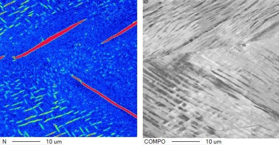
By replacing our old tungsten EPMA by a new FEG-EPMA, OCAS will improve its micro-area analysis capability. The field emission gun (FEG) is capable of achieving a much smaller probe size at lower accelerating voltages and high probe currents over the traditional EPMA with tungsten source. The new FEG-EPMA is additionally equipped with a soft x-ray emission spectrometer for even better detection limits.
OCAS recently installed its brand new FEG-EPMA equipped with an SXES (soft X-ray emission spectrometer). A field emission gun (FEG) typically achieves a probe size 1/2 to 1/8 smaller than a tungsten gun. In addition, the FEG can produce a probe current 20 to 100 times higher than the tungsten (W) gun with the same probe size. As such, a spatial resolution of 0.1 µm can be reached in optimum conditions, compared to 1 µm for a W gun. The new FEG-EPMA has an improved analytical performance combining high lateral resolution and sensitivity.
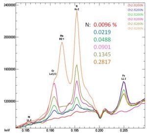
On top, OCAS also invested in a soft X-ray emission spectrometer allowing for the detection of X-rays with energies as low as 50 eV. Which is a 10 fold better energy resolution than WDX and a 5 to 10 times better detection limit. This feature is especially of interest for light elements. The Soft X-Ray Emission Spectrometer (SXES) is an ultra-high resolution spectrometer consisting of a newly-developed diffraction grating and a high-sensitivity X-ray CCD camera. In the same way as EDS, parallel detection is possible, and 0.3 eV (Fermi-edge, Al-L standard) ultra-high energy resolution analysis can be performed, surpassing the energy resolution of WDS.
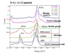
For e.g. nitrogen the chemical bonding state can be analysed from the spectrum peak shape. The peak shapes for nitrates and nitride are completely different, and it is even possible to observe the unique peak shape for ammonium salt, which is very beam sensitive.
The new FEG-EPMA has an extra stable sample stage enabling large scale micro analysis (9×9 cm²).
“The improved features with regard to superior image quality as well as enhanced spatial resolution will enable us to even better visualise sub-micron features and analyse micron size features in a conductive solid material. This opens new doors for research in the field of coating, interface and substrate analysis.”


